TB-8930 · REV F · Technical newsheet
Electronic TestDevice profile
OKI Builds 180-Layer, 15 mm PCB for AI Chip Test Boards
OKI has developed a 180-layer, 15 mm thick PCB aimed at AI semiconductor test equipment, where rising pin counts force deep multilayer test interface boards.
By Sophie Lindqvist3 min read650 words
Features
- OKI developed a PCB with 180 layers for AI semiconductor test equipment
- Finished board thickness is 15 mm, roughly 83 µm per layer
- Application: test boards and interfaces for AI semiconductor devices
- Via architecture, materials, and performance data were not disclosed
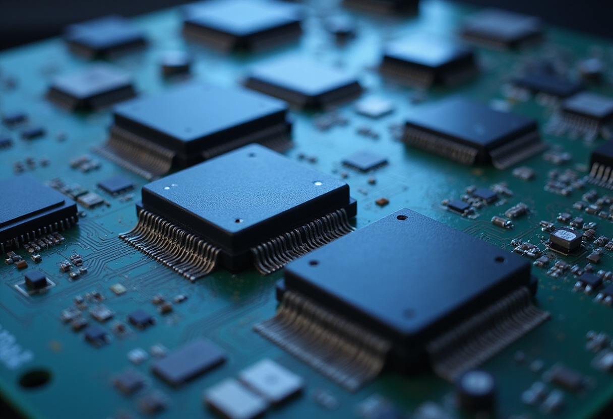
OKI has developed a printed circuit board with 180 layers and a finished thickness of 15 mm, aimed at test equipment used for AI semiconductors. The two numbers define the engineering problem: test boards for AI devices must route thousands of connections between the tester electronics and the device under test, and conventional layer counts force designers into compromises on probe density and signal integrity.
Why AI test hardware needs 180 layers
A burn-in board or test interface board for an AI accelerator or high-pin-count logic device carries one conductive path per pin under test. As AI chips push pin counts upward, the board must stack more signal, ground, and power planes in the same footprint without crosstalk degrading timing measurements at the probe tips. The standard industry response is to add layers and thickness.
OKI's development sits at 180 layers and 15 mm — a thickness-to-layer relationship of roughly 83 µm per layer, which indicates fine-line lamination control rather than simply scaling an existing stack-up. At that aspect ratio, via formation, registration across the stack, and lamination pressure become the yield-limiting steps. The announcement does not specify line width, via pitch, or the dielectric materials used, so measured performance claims should be treated as vendor development statements until test data or qualification results appear.
What the board is for
The target application is test equipment for AI semiconductors — the handler interfaces, socket boards, and device-interface hardware that connect automatic test equipment to the chip. These boards differ from production PCBs in three ways:
- They must survive repeated thermal cycling and mechanical clamping in testers.
- Signal paths must preserve edge rates from the tester's pin electronics to the device socket.
- Layer count grows directly with the channel count of the device under test.
A 180-layer construction signals that OKI is positioning itself at the high end of this niche, where board fabrication capability becomes a gating factor for testing advanced AI devices at all.
Deep stacks change the manufacturing calculus
The physics constraint is straightforward. Every additional layer pair increases registration error accumulated through drilling and lamination. On a 15 mm-thick board, drill aspect ratios climb to the point where conventional through-hole plating reaches its limits, pushing fabricators toward back-drilling, stacked microvias, or buried vias to keep parasitic capacitance out of high-speed paths. OKI has not disclosed which via architecture the board uses, and that omission matters: via strategy largely determines the usable bandwidth of a test interface board, and buyers will need that specification before committing designs.
For test engineers, the relevant questions at adoption time are the ones the announcement leaves open. What is the maximum via aspect ratio OKI can plate reliably at this thickness? What finished-board flatness tolerance does a 15 mm stack hold after reflow-temperature excursions? And what does the layer-count increase do to delivery lead time and cost per board — historically the two variables that decide whether a test organization redesigns around a deep stack or partitions its interface across two thinner boards?
The development also raises a capacity question for the industry. If AI device pin counts keep climbing, test-board fabrication becomes a specialization choke point: relatively few fabricators can produce boards at this layer count with acceptable yield. OKI's entry into that tier gives AI chip test programs an additional qualified source — assuming the company publishes the dimensional and electrical data that ATE engineers will ask for first.
The adoption question
OKI has demonstrated a 180-layer, 15 mm board as a development. The compliance and procurement question it raises: will the company release qualification data — registration tolerance, via reliability under thermal cycling, and impedance control across the stack — soon enough for AI test hardware teams to design it into next-generation interface boards rather than treating it as a capability announcement?
via Google News: Oscilloscopes and test equipment (Source)
Filed under
- pcb
- ai-semiconductors
- test-interface-board
- oki
- signal-integrity
More from Sophie Lindqvist
Show full bio
News editor covering marketplaces and e-commerce at Testbench Report.
66 articles
Application notes
- EU Commission Clears $86M for Semiconductor Test Equipment Site
- AI Chip Demand Drives Record Profits for Taiwan Test Equipment Makers
- China's Seichi Tech Grows Memory-Tester Orders While HBM Win Stays Unverified
- ViTrox Draws Bullish Coverage as AI Inspection Build-Out Accelerates
- Camtek Posts Q1 2026 Earnings Beat on Semiconductor Test Demand